
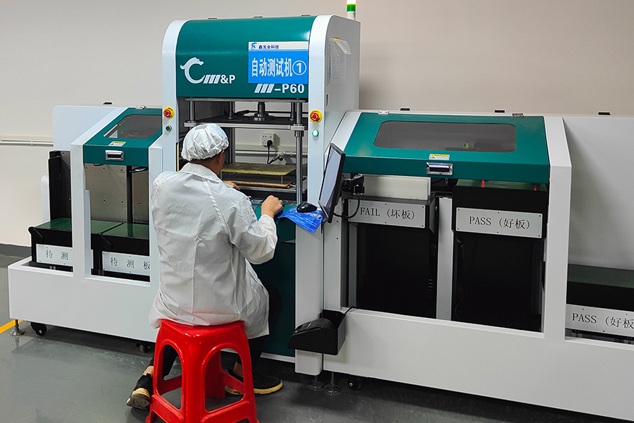
In the fast-evolving world of electronics, creating an LED PCB prototype is essential for developers looking to innovate in lighting solutions. This guide provides detailed insights into the process of prototyping LED PCBs, emphasizing the materials, design strategies, testing methods, and cost-saving techniques involved. By understanding these elements, engineers and manufacturers can streamline their development processes and enhance product performance.
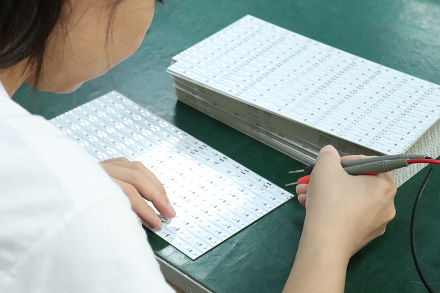
1. What is an LED PCB?
An LED PCB is a printed circuit board specifically designed to accommodate LED components, facilitating efficient lighting solutions in various electronic devices. But here’s the kicker: its design and functionality set LED technology apart from traditional lighting methods. The fundamental difference lies in how LED PCBs manage electrical connections and thermal properties, ensuring optimum performance and longevity of the LEDs themselves.
LED PCBs are utilized in numerous applications, from residential lighting to commercial displays, automotive headlights, and even intricate electronic devices like smartphones. The structure of an LED PCB usually comprises several layers that include a substrate, conductive copper layers, and a solder mask that protects the traces from environmental factors.
What’s the real story? LED PCBs can significantly improve energy efficiency due to their capacity for effective thermal management. This sets them apart from conventional bulbs, which often waste a lot of energy as heat. For example, using an aluminum substrate in LED PCBs not only helps in conducting electricity but also dissipates heat effectively, leading to extended lifespans for the LED components.
Understanding the construction and purpose of LED PCBs is crucial for those looking to prototype effectively. A well-designed PCB can lead to enhanced performance, reliability, and the ability to meet the specific needs of various applications. This knowledge will play a significant role as we delve deeper into the process of prototyping and fabrication.
| Component | Function |
|---|---|
| Substrate | Foundation that supports electrical components |
| Copper Layer | Conducts electricity and distributes power |
| Solder Mask | Protects traces from damage and corrosion |
2. Why is Prototyping Important for LED PCBs?
Prototyping is a crucial step in the development of LED PCBs, allowing designers to test and validate their concepts before committing to mass production. Ready for the good part? The most significant benefit of prototyping is the ability to identify design flaws early in the process, thus avoiding costly mistakes later on.
When creating an LED PCB prototype, engineers can experiment with different materials, layouts, and configurations to find the best combination for performance and efficiency. For instance, a prototype may reveal that a design intended for a specific LED configuration isn’t feasible due to thermal limitations. By identifying this early, redesigns can be made without incurring the expenses associated with full-scale manufacturing.
Moreover, prototyping contributes to cost savings. According to industry studies, effective prototyping can save companies up to 30% in development costs. This fact underscores the value of testing and iterating designs before they go into production, ensuring that the final product meets both consumer demands and technical specifications.
Risk reduction is another key advantage of prototyping. Each prototype serves as a tangible sample of what the end product might be like, allowing stakeholders to evaluate its functionality firsthand. This process helps to ensure that the final product not only meets design specifications but also aligns with user expectations.
Ultimately, the prototyping phase is essential for fostering innovation, enhancing product reliability, and ensuring that the prototypes developed can effectively transition to successful production runs.
| Advantage | Description |
|---|---|
| Design Validation | Early identification of design flaws |
| Cost Savings | Reduces potential expenses in production |
| Risk Reduction | Provides tangible feedback for stakeholders |
3. What Materials are Needed for Prototyping LED PCBs?
Selecting the right materials is vital when prototyping an LED PCB, as these choices can impact the performance, cost, and longevity of the final product. What’s the real story? High-quality materials not only enhance the durability of PCBs but also improve their overall functionality.
Common choices for LED PCB substrates include FR-4 laminates and aluminum. FR-4 is a glass-reinforced epoxy laminate that is inexpensive and widely used. It provides excellent electrical insulation, making it suitable for many standard applications. However, when heat dissipation is a critical factor, aluminum substrates become a preferred choice due to their superior thermal conductivity. This leads to better performance in high-power LED applications, such as automotive lighting or commercial displays.
In addition to the substrate, conductive copper layers must be of high quality to ensure efficient electrical transfer. Poor-quality copper can lead to increased resistive losses, which in turn heat generates unnecessary waste energy. Moreover, the solder mask used must be durable enough to withstand the manufacturing process and environmental factors, providing an effective barrier against oxidation.
What’s more, there are also advanced materials like polyimide and various composites emerging in the industry, which offer both thermal and electrical benefits. These materials cater to specialized applications where performance demands are heightened or where traditional materials may not suffice.
Selecting the right materials will not only optimize the LED PCB prototype but can also define its ultimate success in the marketplace. Therefore, careful consideration and selection of materials based on application requirements are essential for maximizing performance.
| Material Type | Purpose |
|---|---|
| FR-4 | Cost-effective and widely used substrate |
| Aluminum | Superior thermal conductivity for better heat dissipation |
| Copper | Conducts electricity efficiently |
4. How to Design an LED PCB Prototype?
Designing an efficient LED PCB prototype involves several well-defined steps. But here’s the kicker: overlooking any step can lead to complications later on, affecting functionality and increasing costs. The first step begins with understanding the specifications of the LEDs you intend to use. This includes their voltage, current rating, and power requirements, all of which will significantly impact your PCB design.
Once you have established these requirements, the next phase is to use PCB design software to create the layout. Popular software options include Eagle, KiCAD, and Altium Designer, each offering a range of tools and features tailored for PCB development. You must accurately place components within the layout, ensuring that all connections align with the schematic drawn earlier.
But that’s not all—thermal management must also be a key consideration during the layout process. Placing components that generate heat, such as high-power LEDs, should be done thoughtfully to prevent overheating. Utilizing thermal vias and heat sinks in your design can mitigate potential heat issues and improve durability and performance.
Additionally, trace width and layout should be optimized to handle the required current without overheating. Wider traces reduce resistance and improve electrical performance, while also aiding in heat dissipation.
After designing, conduct design rule checks (DRCs) to identify any potential problems, and then move on to creating a prototype based on the finalized design. The prototyping phase provides the opportunity to test and validate your design, leading to insights that can improve the final product.
| Design Element | Importance |
|---|---|
| LED Specifications | Influence overall design and power needs |
| PCB Design Software | Enables accurate layouts and efficient designs |
| Thermal Management | Prevents overheating and ensures component longevity |
5. What Are the Key Specifications for LED PCB Design?
Understanding key specifications for LED PCB design is crucial for achieving optimal performance. What’s the real story? The specifications dictate not only the efficiency of the LEDs but also the reliability of the entire lighting system.
First, voltage and current ratings are paramount in any LED PCB design. Each LED operates within a specific voltage range, and exceeding this can lead to failure. When designing your PCB, ensure that the supply voltage matches the maximum forward voltage of the LEDs. This is critical to preventing damage and ensuring longevity.
Furthermore, size and thickness of the PCB are vital considerations. The size must accommodate the number of LEDs and other components while fitting within the desired product dimensions. Thicker boards often provide better structural integrity, but they also add to manufacturing costs.
Thermal management is another essential specification. Ensure that thermal vias, copper pours, and heat sinks are part of your design if the LEDs will generate significant heat. This will prevent overheating and failure, improving the reliability of the lights over time.
Lastly, consider the impedance of traces on the PCB, especially if high-frequency signals are involved. Proper trace width and spacing will help reduce signal loss and ensure performance efficiency.
Whether you’re creating residential lighting or high-intensity commercial solutions, adhering to these specifications ensures that your LED PCB performs at its best and remains cost-effective.
| Specification | Importance |
|---|---|
| Voltage/Current | Key determinants of LED functionality |
| Size/Thickness | Affects design compatibility and costs |
| Thermal Management | Prevents overheating and enhances reliability |
6. How to Create the Schematic for Your LED PCB?
Creating a schematic for your LED PCB is a foundational step in the design process. Ready for the good part? A well-structured schematic serves as a blueprint for PCB layout, ensuring that every connection is clear and logically defined. Start by carefully selecting the components you will use, from the LEDs themselves to resistors and capacitors needed for the circuit.
Using PCB design software, you can create a clear visual representation of how these components will connect. In this schematic, label each component and specify its parameters, such as values for resistors. This attention to detail makes it easier for manufacturers to understand your design.
One important aspect to consider is how to handle current limiting. Resistors may need to be included alongside your LED components to prevent excess current that can lead to LED failure. It’s essential to calculate the correct resistor values based on your power specifications, ensuring that the circuit operates effectively.
Additionally, ensure that your schematic adheres to best practices in schematic design. This means utilizing standardized symbols for components, maintaining a logical flow of connections, and avoiding confusing crossovers that may complicate the layout process.
After completing your schematic, run design checks to catch any possible errors. Once verified, this schematic will serve as the foundation for your PCB layout, ensuring a smooth transition to the manufacturing phase.
| Schematic Element | Role in Design |
|---|---|
| Components | Building blocks of your circuit |
| Resistors | Essential for current management |
| Standard Symbols | Ensures clarity and uniformity in design |
7. How is the PCB Fabrication Process Executed?
PCB fabrication is a critical step that transforms your design from a concept to a physical product. But here’s the kicker: understanding this process helps you manage expectations and collaborate effectively with manufacturers. The first phase in fabrication begins once you submit your Gerber files—these files detail the design layers, including the copper traces, solder mask, and silkscreen layers.
Next comes material selection. Fabricators will choose appropriate substrates based on your specifications, with FR-4 being a common choice for general applications, while aluminum substrates may be selected for high-power LED applications.
Once the materials are prepared, the PCB manufacturing process involves several steps, including etching, drilling, and plating. Etching involves removing unwanted copper from the surface of the board to create the needed pathways for electrical connectivity. Drilling is then performed to create holes for the component leads.
After drilling, the board is typically plated, which improves conductivity and prepares the surface for the solder mask application. The solder mask protects the copper traces from oxidation and prevents solder from bridging adjacent tracks. Finally, a silkscreen process labels component positions and provides further customer information.
Quality control is vital throughout each of these steps. Fabricators often conduct various tests, including electrical tests, to ensure the board is free from defects. This attention to detail during the fabrication phase results in a quality product ready for assembly.
| Fabrication Step | Description |
|---|---|
| Material Selection | Determines the base for your PCB |
| Etching | Creates the conductive pathways |
| Drilling | Prepares for component placement |
8. What Does the Assembly Process for LED PCBs Look Like?
The assembly of LED PCBs is crucial for ensuring that your design functions correctly once fabricated. What’s the real story? This process involves several methodical steps that guarantee the effective attachment of components to the PCB. The first step begins with a thorough cleaning of the PCB to remove any residues from fabrication. Any contaminants left on the board can interfere with soldering and overall performance.
Next, position the components on the PCB as per the schematic. Utilizing a pick-and-place machine can enhance accuracy and speed, particularly for high-volume production. For smaller runs, manual placement may suffice, but care should be taken to ensure correct orientation and positioning.
Once all components are correctly placed, the PCB must undergo soldering. Depending on the type of components being used, either reflow soldering for surface-mounted devices or wave soldering for through-hole components can be employed. Ensure the soldering technique used is appropriate for the heat sensitivity of the components—especially important with LED technology that can be damaged by excess heat.
After soldering, implementation of a visual inspection is necessary. Examine the board for solder quality, proper component placement, and any potential shorts. Following visual inspections, testing the assembled PCB is crucial. Electrical testing can ensure that all connections are functional and that the board is ready for deployment.
Ultimately, a methodical approach to assembly is vital for ensuring product reliability and performance, setting the stage for successful deployment.
| Assembly Step | Purpose |
|---|---|
| Cleaning | Ensures no residue interferes with soldering |
| Component Placement | Accurate positioning is essential |
| Soldering | Attaching components securely to the board |
9. How to Test Your LED PCB Prototype?
Testing your LED PCB prototype is essential for validating its functionality and ensuring that it meets performance specifications. Ready for the good part? There are several key testing methods to employ, each addressing different aspects of your PCB’s performance.
First and foremost is visual inspection. This involves checking the assembly process for elevated solder joints, misplaced components, and any visible damage. A thorough visual inspection can identify a range of issues, from simple errors to more complex defects that could hinder performance.
Electrical testing follows visual inspection, focusing specifically on measuring current, voltage, and resistance across various points on the PCB. This can help spot discrepancies from intended values, indicating potential issues within the circuit. Common tools for this purpose include multimeters and oscilloscopes, both of which provide valuable insights into the board’s performance.
Thermal testing is also critical, particularly in LED applications where managing heat is vital for longevity. It’s not uncommon to utilize thermal cameras to monitor temperatures during operation, ensuring they remain within safe limits.
Ultimately, testing isn’t just about finding faults; it’s an opportunity to collect data that can inform future iterations of your design. By assessing prototype performance comprehensively, you can enhance reliability and efficiency, paving the way for successful production runs.
| Testing Technique | Purpose |
|---|---|
| Visual Inspection | Identifies assembly and component issues |
| Electrical Testing | Measures circuit functionality |
| Thermal Testing | Ensures heat management is adequate |
10. What Troubleshooting Methods Are Effective for LED PCBs?
When problems arise with your LED PCB, troubleshooting is key to getting things back on track. This is where it gets interesting: a systematic approach to troubleshooting can save time and resources. The first step typically involves a thorough visual inspection. Look for obvious signs of damage, such as burnt components, lifted pads, or poor solder joints. Identifying visible issues can often lead straight to the source of the problem.
Next, electrical testing comes into play. Use a multimeter to check for continuity across the various traces and components. This helps uncover issues such as broken connections or components that aren’t functioning correctly. If voltage levels are lower than expected, it may indicate a faulty power supply, a short circuit, or a poorly designed trace.
If electrical testing doesn’t yield answers, thermal profiling during operation can reveal hidden issues. Excessive heat in specific components may indicate they are being over-driven or are improperly matched to the circuit design.
If you’re still unable to resolve the problem, consider seeking input from experienced colleagues or industry professionals. They can provide fresh perspectives and may be familiar with issues that aren’t readily apparent. Gathering diverse insights can often lead to quicker resolutions.
Ultimately, an organized troubleshooting process can help address any inconvenience efficiently, ensuring that LED PCBs deliver the performance and reliability expected.
| Troubleshooting Step | Description |
|---|---|
| Visual Inspection | Check for visible defects or damage |
| Electrical Testing | Diagnose connectivity and functionality |
| Thermal Profiling | Monitor temperature for hotspots |
11. What Are Some Best Practices for Maintaining LED PCBs?
Maintaining LED PCBs is essential for ensuring they continue to perform optimally throughout their lifespan. Ready for the good part? Regular maintenance practices can lead to improved reliability and longevity. Begin with routine inspections of the physical condition of the PCB. Look for signs of wear or damage, such as discoloration, corrosion, or broken connections.
Cleaning the PCB is another key aspect of maintenance. Dust and grime can accumulate over time, contributing to overheating or impacting performance. It’s advisable to use isopropyl alcohol and a soft brush to gently clean the surface of the board and its components without causing damage.
Monitoring operating temperatures is crucial, particularly since heat buildup can drastically reduce the lifespan of LEDs. Using thermal sensors can help track temperatures over time to ensure they remain within acceptable limits. If temperatures are frequently too high, consider revisiting the thermal management strategy to identify possible improvements.
Documenting maintenance activities is equally important. Detail each inspection, cleaning session, and any repairs made, creating a comprehensive history for each PCB. This record can serve as a valuable resource for identifying patterns or recurring issues.
Adhering to these best practices not only enhances the performance of LED PCBs but also ensures that they will continue to meet user expectations for many years.
| Maintenance Task | Importance |
|---|---|
| Routine Inspections | Identifies potential issues early |
| Cleaning | Prevents overheating and ensures efficiency |
| Temperature Monitoring | Maintains performance and longevity |
12. How to Scale Up from Prototype to Production?
Transitioning from an LED PCB prototype to full-scale production involves strategic planning and coordination. What’s the real story? Successfully scaling requires careful consideration of factors that can affect manufacturing efficiency and product quality.
The first step is assessing your prototype results. Analyze performance data to determine if design adjustments are needed before moving to production. This phase might include revising the BOM (Bill of Materials) to better align with performance metrics and cost goals.
Next, finalize the production setup with your chosen manufacturer. Communication here is key. Ensure that the manufacturer fully understands your requirements, including specifications, materials, and quality expectations. Establish a timeline that accounts for both production flows and any potential downtimes.
Quality assurance measures become even more critical in production. Implement checks at various stages of manufacturing to maintain consistency and reliability. Statistical Process Control (SPC) techniques can help monitor processes in real time, identifying areas for improvement before they lead to defects.
Finally, plan for logistics and distribution. This includes managing inventory levels to ensure timely delivery, especially if demand is expected to fluctuate. Having a robust plan in place ensures that your LED PCB reaches the market quickly and efficiently, facilitating overall business success.
| Scaling Step | Importance |
|---|---|
| Prototype Review | Ensures required adjustments are made before production |
| Manufacturer Coordination | Maintains clarity and quality expectations |
| Quality Assurance | Essential for consistency and reliability |
13. What Are the Cost Factors Involved in LED PCB Prototyping?
Understanding cost factors is crucial for budgeting in LED PCB prototyping. Ready for the good part? Various elements come into play when calculating expenses. Material costs are often the most significant component of the budget. High-quality substrates, such as aluminum, tend to be more expensive than standard options, but they significantly contribute to a PCB’s functionality and durability.
Next, consider the complexity of the design. More intricate layouts with multiple layers can lead to increased fabrication and assembly costs. FOil intensive designs may also lead to an uptick in PCB manufacturing expenses. Trade-offs between performance and cost must be evaluated carefully.
Additionally, the chosen manufacturing method will impact costs. Small batch runs can be more expensive on a per-unit basis than larger quantities. If demand is high, it may be cost-effective to move quickly to full production, as economies of scale will lower the overall cost per unit.
Testing and validation expenses are also important to account for during the prototyping phase. Ensuring each board meets stringent performance metrics requires adequate resources dedicated to thorough testing and quality control processes.
By understanding and anticipating these cost factors, companies can create an effective budget that supports a successful prototyping and production process while allowing room for adjustments as needed.
| Cost Factor | Description |
|---|---|
| Material Costs | Influences overall project expenses |
| Design Complexity | Impacts fabrication and assembly pricing |
| Testing Expenses | Ensures reliable performance and quality |
14. How to Stay Updated on LED PCB Technology Trends?
Keeping abreast of the latest trends in LED PCB technology is essential for professionals in the field. What’s the real story? The rapid evolution of technology means staying informed is not just an option; it’s a necessity for success. One of the best ways to do this is by subscribing to industry journals and online publications dedicated to PCBs and LED innovations. These resources often provide insights into new materials, design techniques, and emerging best practices.
Networking at industry conferences is another effective method to gain knowledge. Events such as PCB West and the IPC APEX Expo offer networking opportunities, educational sessions, and workshops that explore the latest technologies and challenges in the industry. Engaging with peers can stimulate fruitful discussions and collaborations that benefit your work.
Moreover, joining online forums and professional organizations dedicated to electronics and PCB design can connect you with thought leaders and innovators. These platforms offer ample opportunities for knowledge sharing and problem-solving.
Keeping an eye on regulatory changes is also critical. As sustainability becomes increasingly important in manufacturing practices, staying updated on regulations and standards can help you adapt quickly and responsibly. Embracing these changes will provide you with a competitive edge.
By continually seeking out and sharing knowledge, professionals in the LED PCB space can enhance their expertise and drive innovation in their projects.
| Information Source | Type |
|---|---|
| Industry Journals | Provides insights into new technologies |
| Conferences | Opportunities for networking and discovery |
| Online Forums | Platforms for knowledge sharing and problem-solving |
15. What Future Trends Can We Expect in LED PCB Development?
The future of LED PCBs promises exciting developments that may redefine the landscape. Ready for the good part? Innovations in materials, design, and applications are on the horizon. One prominent trend is the use of advanced, eco-friendly materials that not only meet performance criteria but also align with growing sustainability efforts. This shift could lead to reduced environmental impacts throughout the lifecycle of PCB production.
Another significant change on the horizon is the integration of smart technologies into LED lighting. As the Internet of Things (IoT) continues to expand, more LED applications will combine connectivity, enabling real-time monitoring and responsiveness. This would allow lighting solutions to adapt to user needs and improve energy efficiency in remarkable ways.
Furthermore, the focus on health and well-being will lead to the rise of human-centric lighting solutions, where LED technologies adjust light spectrums and intensity based on natural light conditions and user preferences.
Finally, increased automation in PCB production processes is likely to improve efficiency and consistency in manufacturing, allowing for faster turnarounds and reduced costs.
In conclusion, the future of LED PCB development is bright, with innovative technologies promising to enhance both performance and sustainability in lighting solutions.
| Trend | Description |
|---|---|
| Eco-Friendly Materials | Aligns with sustainability goals |
| Smart Technology Integration | Enables real-time monitoring and efficiency |
| Human-Centric Solutions | Focuses on user health and well-being |
Conclusion
Easily prototyping your LED PCB is a profound step that encompasses understanding materials, design considerations, and fabrication processes. Throughout this guide, we’ve explored the necessity of each phase—from conceptual design to scaling production—emphasizing the significance of proper testing, maintenance, and updating technology. By adhering to the outlined strategies, professionals can navigate the complexities of LED PCB prototyping effectively, paving the way for innovative applications that meet both market and consumer demands.
FAQ Section
Q1: What is an LED PCB?
An LED PCB is a printed circuit board specifically designed to accommodate LED components, facilitating efficient lighting solutions in various electronic devices.
Q2: How does the prototyping process work for LED PCBs?
Prototyping involves designing a preliminary version of an LED PCB, fabricating it, assembling components, and testing it to ensure functionality and performance before mass production.
Q3: What materials are commonly used in LED PCB prototypes?
Common materials include FR-4, aluminum, and copper, which are chosen based on thermal performance, electrical conductivity, and cost efficiency.
Q4: How can I troubleshoot issues with my LED PCB?
Troubleshooting involves checking connections, testing voltage and current levels, and using diagnostic tools to identify faulty components.
Q5: What are some best practices for maintaining LED PCBs?
Best practices include routine inspections, keeping them clean, monitoring temperature, and maintaining detailed documentation of all maintenance activities.