
Understanding LED PCBs is essential for anyone involved in electronics and lighting solutions. These technologically advanced components allow for efficient lighting and versatile designs in myriad applications. This article will explore the definition, significance, materials, design, specifications, assembly, testing, and future trends of LED PCBs. By the end of this guide, readers will have a comprehensive understanding of LED PCBs and their critical role in modern technology.
1. What Are LED PCBs?
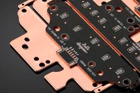
LED PCBs, or light-emitting diode printed circuit boards, are designed specifically to support LED components. But here’s the kicker: unlike traditional printed circuit boards, LED PCBs are optimized not only for electrical functionality but also for thermal management. They typically encapsulate multiple layers, including a substrate that can either be fiberglass or aluminum, providing both electrical conductivity and heat dissipation required by high-power LEDs.
What’s the real story? The structure of an LED PCB usually consists of a copper layer, insulating materials, and a protective solder mask on top. These components work in conjunction to ensure that the LEDs function correctly while also managing the heat generated during operation.
In practical terms, LED PCBs are commonly found in a range of applications, from consumer electronics like televisions and smartphones to industrial lighting and automotive headlights. This versatility is bolstered by improvements in their design, allowing for compact configurations and integrated circuitry that can support diverse lighting designs.
Understanding the intricacies of LED PCBs can significantly impact design choices, influencing everything from cost to efficiency. This is vital knowledge for anyone involved in electronics or lighting solutions, as the choice of PCB can make or break a product’s performance.
| Feature | Description |
|---|---|
| Material | Typically fiberglass or aluminum |
| Layers | Copper layer, insulating materials, solder mask |
| Application | Consumer electronics, industrial lighting, automotive |
2. Why Are LED PCBs Important?
LED PCBs are critical for several reasons. What’s the real story? The importance of LED PCBs lies not only in their ability to provide efficient lighting but also in their role in energy conservation and sustainability. In recent years, the shift from incandescent to LED lighting has been pivotal in reducing energy consumption, and LED PCBs are a cornerstone of this transition.
Additionally, the applications of LED PCBs extend far beyond traditional lighting solutions. For instance, in the automotive industry, LED PCBs are used in headlights, taillights, and dashboard indicators, often integrating various lighting functions into a single unit. This integration is made possible due to the flexibility in design that LED PCBs provide.
Another significant benefit of LED PCBs is their energy efficiency. They consume less power while delivering the same, if not greater, light output compared to older technologies. For example, research indicates that switching to LED lighting can reduce energy use by approximately 75%. In terms of economic impact, this translates to lower utility bills and extended product lifespans, which ultimately enhances profitability for manufacturers.
Don’t overlook the environmental impact. LED lights produce less heat than traditional bulbs, reducing cooling requirements in indoor settings and diminishing the overall carbon footprint. This environmental aspect makes LED PCBs an ideal choice for sustainable development.
| Significance | Description |
|---|---|
| Energy Efficiency | Substantially lower power consumption |
| Versatility | Applicability in various industries |
| Environmental Impact | Reduced carbon footprint and energy conservation |
3. What Materials Are Used in LED PCBs?
Choosing the right materials for LED PCBs is paramount for performance and longevity. But here’s the kicker: not all materials are created equal, especially when it comes to heat management and electrical conductivity. The common choice for substrates is FR-4, a fiberglass laminate that is effective for standard applications. But many applications require materials that can handle more substantial heat, such as aluminum, which is preferred due to its superior thermal conductivity.
What’s the real story? The choice of copper thickness is also critical. Thicker copper layers (like 2 oz or more) enhance thermal dissipation and allow for better current handling. Many manufacturers often prefer using double-sided copper PCBs for complex LED circuit configurations, as they provide more efficient pathways for electricity and heat exchange.
Furthermore, protective coatings play a vital role. A solder mask not only protects the copper traces from moisture and oxidation but also prevents solder bridging during assembly, which can be crucial in densely packed circuits typical of LED designs. Some manufacturers also opt for thermal interface materials, ensuring effective heat transfer from the LED chips to the PCB.
Finally, advancements in materials science are leading to innovations such as flexible PCBs, which can be particularly useful in applications where adaptability is essential. This flexibility allows for unique installation solutions, especially in compact devices that require specialized lighting systems.
| Material Type | Purpose |
|---|---|
| FR-4 | Standard substrate for PCB construction |
| Aluminum | Superior thermal conductivity for heat dissipation |
| Copper Thickness | Influences thermal and electrical performance |
4. How Does the Design Process for LED PCBs Work?
The design process for LED PCBs is a multifaceted venture that requires careful planning and expertise. Ready for the good part? It all begins with understanding the specific needs of the LED applications, including power requirements and spatial considerations.
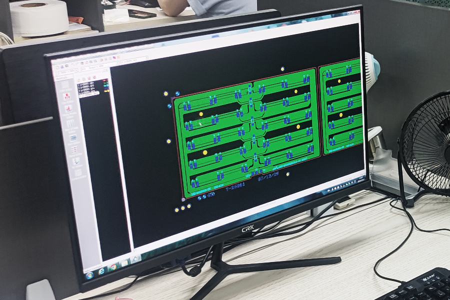
Design software plays a crucial role in this stage. Tools like Altium Designer, KiCAD, and Eagle allow engineers to construct, simulate, and validate their designs before fabrication. A well-crafted schematic diagram is essential, detailing component placement, connections, and other design parameters. From there, engineers can draft the layout, making decisions about trace widths and placement to ensure optimal signal integrity and heat dissipation.
Thermal management also demands attention during the design stage. Designers must account for heat sinks and thermal vias to ensure properly regulated temperatures across the PCB, preventing damage to LED components.
What’s the real story? Design considerations extend beyond just electrical functionality. For example, aesthetics and physical form are also important, especially in consumer products where design plays a significant role. LED PCBs often integrate seamlessly into the overall product design, ensuring they contribute to both appearance and function.
Finally, once the design is complete, it undergoes a series of simulations and checks to validate performance against specified metrics. This crucial phase is where potential design flaws are identified and corrected before moving forward to fabrication.
| Design Component | Importance |
|---|---|
| Schematic Diagram | Basis for the entire PCB layout |
| Thermal Management | Ensures LED longevity and optimal performance |
| Simulation & Checks | Validates design against required specifications |
5. What Key Specifications Should You Consider?
When designing LED PCBs, several key specifications must be taken into account. But here’s the kicker: overlooking these aspects can lead to product failure or inefficiency.
First and foremost are voltage and current requirements. Each LED component has a specific forward voltage and current threshold, and designing the circuit to accommodate these specifications is essential for optimal performance. Properly calculated resistor values and voltage levels are crucial to prevent early LED failure.
Size and thickness of the PCB are also critical factors. The dimensions dictate not only the space for components but also the overall footprint of the final product. Thicker PCBs can offer better manufacturability and rigidity, but also come with increased costs.
Thermal management specifications cannot be overlooked. As mentioned previously, LED components generate heat, and if not managed properly, it can lead to performance issues or even failure. Designers must incorporate heat sinks or thermal vias and ensure the board layout promotes good airflow.
Lastly, trace widths should be considered, as these affect the electrical performance of the PCB. Wider traces can handle higher currents, reducing the risk of overheating while also contributing to the overall reliability of the board.
| Specification | Importance |
|---|---|
| Voltage/Current | Key determinants of LED functionality |
| Size/Thickness | Impacts design versatility and manufacturing costs |
| Thermal Management | Prevents overheating, ensuring long-term reliability |
6. How to Create a Schematic for an LED PCB?
Creating a schematic for an LED PCB is a critical step that lays the groundwork for the entire design. Ready for the good part? It begins by selecting the appropriate components based on the desired specifications, including LEDs, resistors, capacitors, and any other necessary circuitry.
Next, using PCB design software, the schematic is constructed to represent how these components will interact. This includes placing components strategically and specifying their connections. Every component must be accurately labeled to facilitate the assembly process.
What’s the real story? Consideration of current limiting is essential in this stage. Resistors may need to be included to prevent excess current, ultimately protecting the LEDs from damage. It’s vital to calculate precise resistance values based on the system’s power requirements to ensure the circuit operates effectively.
Best practices for schematic creation also involve using standardized digital symbols and ensuring a clear layout. This minimizes confusion during both the design phase and subsequent assembly stages. Employing design rules within the software can help identify potential errors early on, ensuring a high-quality schematic.
After the schematic is drafted, it must be reviewed and validated to ensure all connections are accurate and compatible with the PCB layout. One common technique is to run Electrical Rule Checks (ERC) within the software, which can pinpoint conflicts or issues that must be addressed.
| Schematic Component | Role in Design |
|---|---|
| LEDs | Primary light source within the circuit |
| Resistors | Limiting current to protect components |
| Digital Symbols | Enhances readability and standardization |
7. What Is the PCB Fabrication Process?
The PCB fabrication process is where your design transforms into a tangible product. But here’s the kicker: this step includes several stages, all of which require precision and attention to detail to ensure high-quality results.
The process begins once the finalized design files, typically Gerber files, are submitted to the manufacturer. These files provide a detailed layout of the PCB, including layer information, trace dimensions, and hole specifications.
What’s the real story? The first step in fabrication is choosing the appropriate materials, based on the discussed specifications. Next, the PCB undergoes a series of essential processes: etching where unwanted copper is removed, drilling where holes are created for component leads, and plating where copper is added to enhance conductivity.
Following these initial steps, a solder mask is applied to protect the board from environmental damage and prevent solder bridges during assembly. The final stage involves applying a silkscreen layer that labels the component locations, aiding in assembly and troubleshooting.
Quality control is critical at every stage of fabrication. Manufacturers frequently conduct inspections and tests to ensure that every PCB meets the required specifications and performance metrics. This ensures the final product is robust and reliable.
| Fabrication Step | Description |
|---|---|
| Choosing Materials | Ensures proper substrate and trace characteristics |
| Etching | Creates the conductive pathways on the PCB |
| Solder Masking | Protects copper traces and prevents solder bridging |
8. How Do You Assemble LED PCBs?
Assembling LED PCBs is a meticulous process that combines various techniques to ensure all components function correctly. What’s the real story? The assembly process can significantly influence the overall quality and reliability of the finished product, so attention to detail is essential.
The first step in assembly is a thorough cleaning of the PCBs to remove any contaminants left from the fabrication process. This ensures that soldering will perform optimally and that components can adhere properly.
Next, components are placed onto the PCB. This can be done manually or with the assistance of automated pick-and-place machinery, which enhances accuracy and speed, especially for mass production runs. Regardless of the method used, attention must be paid to ensure that each component is oriented properly to prevent assembly errors.
Once all components are positioned, the soldering process begins. For surface-mounted components, reflow soldering is typically used, which involves applying solder paste and heating the PCB to melt the solder onto the components. For through-hole components, wave soldering or hand soldering methods may be utilized.
After soldering, inspection is critical. Visual inspections look for solder quality, correct placement, and any potential defects. Following this, functional testing validates that all components are working as designed, ensuring a reliable final product.
| Assembly Step | Importance |
|---|---|
| Cleaning | Prevents contamination that can affect soldering |
| Component Placement | Ensures accurate positioning for assembly |
| Inspection | Validates assembly quality and identifies issues |
9. What Testing Methods Are Used for LED PCBs?
Testing LED PCBs is essential for validating their performance and ensuring reliability. Ready for the good part? There are various testing methodologies, each addressing different aspects of a PCB’s functionality.
The first step typically involves visual inspection. This preliminary assessment checks for solder defects, misaligned components, and potential physical damage. It’s an invaluable step that provides instant feedback about potential issues that could affect performance.
Electrical testing follows visual inspection and may include continuity tests to confirm that signals are properly routed between components. Multimeters and oscilloscopes are commonly utilized to measure voltage, current, and resistance levels throughout the circuit.
Thermal testing is crucial, especially for LED applications. The heat generated by operating LEDs must be monitored closely to ensure temperatures remain within safe limits. Thermal imaging cameras can reveal hotspots that may indicate poor performance or design flaws.
On top of this, it’s also advisable to run specific functional tests based on the LED PCB’s application. For example, in lighting systems, testing lumens output and color accuracy ensures the design meets consumer and industry expectations.
| Testing Method | Purpose |
|---|---|
| Visual Inspection | Identifies physical defects and solder issues |
| Electrical Testing | Validates circuit connections and performance |
| Thermal Testing | Ensures LED components operate within safe limits |
10. How Can You Troubleshoot Issues with LED PCBs?
Troubleshooting LED PCBs when issues arise is an integral part of maintaining their performance. What’s the real story? A systematic approach to troubleshooting can reveal the roots of most problems without wasting time and resources.
The first step in the troubleshooting process usually involves a detailed visual inspection. Look for obvious signs like burnt components, lifted pads, or unsoldered connections. Identifying visible flaws can help narrow down the root cause of circuit failure.
Next, focus on electrical testing. Utilize a multimeter to evaluate continuity across different traces and components. This will help highlight any problematic areas within the circuit. If discrepancies are noted, further investigation into specific components may be necessary.
It may also be useful to perform functional tests. Check whether the LEDs are illuminating as expected or if there are variations in brightness across the array. These tests may bring other underlying issues to light.
Should these troubleshooting methods not yield satisfactory results, consider consulting with experienced engineers or peers in the industry. Sometimes, a fresh perspective can identify issues you may have initially overlooked.
| Troubleshooting Step | Explanation |
|---|---|
| Visual Inspection | Identifies apparent issues and damages |
| Electrical Testing | Diagnoses connection failures and performance |
| Functional Testing | Assesses LED performance against specifications |
11. What Are Some Best Practices for Maintaining LED PCBs?
Maintaining LED PCBs is crucial to ensuring they function correctly and have a long lifespan. But here’s the kicker: regular maintenance can significantly enhance reliability and performance.
Routine inspections should be scheduled to evaluate the physical condition of the PCB. Looking for signs of wear, corrosion, or damage can prevent minor issues from becoming costly failures. Regular visual checks should follow good maintenance practices to ensure adherence.
Cleaning is another essential aspect of PCB maintenance. Accumulated dust and grime can interfere with electrical performance by causing overheating. Cleaning with isopropyl alcohol and a soft brush can effectively remove contaminants without damaging delicate components.
Temperature monitoring is vital in maintaining LED PCBs, given their susceptibility to heat. Hot spots can dramatically shorten the life of LEDs, so employing thermal sensors for consistent monitoring can alert users to potential overheating problems before they lead to catastrophic failure.
Finally, documenting all maintenance activities is helpful. Comprehensive records include inspections, repairs, and cleaning sessions, aiding in identifying patterns or recurring issues, ultimately leading to improved performance.
| Maintenance Task | Importance |
|---|---|
| Routine Inspections | Early identification of potential issues |
| Cleaning | Prevents performance degradation and overheating |
| Temperature Monitoring | Ensures LEDs operate within safe limits |
12. How to Scale Up from Prototype to Production?
Transitioning from an LED PCB prototype to full-scale production requires careful planning and coordination. What’s the real story? Successful scaling hinges on evaluating the prototype results and ensuring that all elements are ready for mass manufacturing.
Initially, review the performance metrics from the prototype phase. Analyzing feedback will help identify any design modifications or enhancements needed before moving forward. This data-driven approach minimizes the risk of product failures once production commences.
Next, collaborate closely with your manufacturing partner. Clear communication is pivotal to ensure that they understand the specifications, materials, and quality expectations. Arrange for trial runs to verify production processes and establish timelines that account for potential delays.
Implement quality assurance measures throughout production. Regular inspections and testing should occur at multiple production stages to maintain the highest quality standards. Establishing Statistical Process Control (SPC) techniques can assist in monitoring processes in real-time.
Lastly, plan for logistics and distribution carefully. Ensuring that your product reaches its consumers efficiently while managing inventory effectively is crucial. A robust supply chain can significantly impact overall business success, especially after transitioning from prototypes to full-scale production.
| Scaling Step | Importance |
|---|---|
| Performance Review | Identifies necessary adjustments before scaling |
| Manufacturer Collaboration | Ensures quality and timeline adherence |
| Logistics Planning | Ensures timely delivery and inventory management |
13. What Are the Cost Considerations for LED PCBs?
When budgeting for LED PCBs, it is crucial to account for various cost factors. But here’s the kicker: understanding these costs can lead to better decision-making and ultimately more successful projects.
Material costs typically comprise a significant portion of the overall budget. High-quality materials for substrates, copper layers, and protective coatings often lead to higher initial costs, but they can yield better long-term performance and durability.
Labor and production expenses can also vary based on the complexity of the design. For example, designs with multiple layers will increase labor costs during both fabrication and assembly, impacting the overall budget.
Another important aspect is testing and quality assurance. Properly verifying that each LED PCB meets performance specifications requires time and resources. This testing can significantly influence financial planning, particularly for projects requiring rigorous standards.
Consideration of unforeseen expenses is also necessary. Unexpected issues during development or production can result in additional costs, so it’s wise to allocate a financial buffer in the budget to mitigate unexpected challenges.
| Cost Factor | Description |
|---|---|
| Material Costs | Main component of overall budget |
| Labor/Production | Increases with complexity of PCB design |
| Testing Expenses | Essential for ensuring reliability and performance |
14. How to Stay Updated on LED PCB Trends?
Keeping updated on LED PCB trends is vital for professionals in the field. What’s the real story? The fast-paced nature of technology means that continual learning is essential for maintaining a competitive edge.
Subscribing to industry publications and online journals is a great way to stay informed. These resources often provide valuable insights into new technologies, materials, and methods emerging within the LED PCB space.
Attending industry conferences is another effective strategy for staying connected. Events like PCB West or IPC APEX Expo offer networking opportunities and feature educational sessions on the latest trends and developments. Engaging with peers at these events can lead to collaborations and new insights.
Online forums and professional organizations provide additional platforms for networking and knowledge sharing. Engaging in discussions can expose participants to different perspectives and innovative ideas.
Lastly, keeping abreast of regulatory changes and sustainability trends is crucial. As consumers and businesses become increasingly aware of environmental impacts, being informed about industry standards helps ensure compliance and the ability to meet consumer demand for sustainable products.
| Information Source | Purpose |
|---|---|
| Industry Publications | Keeps professionals informed of latest trends |
| Conferences | Networking and educational opportunities |
| Online Forums | Offers platforms for knowledge sharing |
15. What Future Developments Can We Expect in LED PCBs?
The future of LED PCBs looks promising, with numerous innovations and trends on the horizon. Ready for the good part? Advancements in materials science are paving the way for sustainable solutions that will redefine the landscape of PCB manufacturing.
Eco-friendly materials are at the forefront of this evolution. As the demand for sustainability grows, manufacturers are exploring alternative substrates and components that minimize environmental impact while retaining performance.
Integration of smart technologies into LED PCBs is another exciting trend. The Internet of Things (IoT) continues to proliferate, and LED PCBs will increasingly feature connectivity that enhances functionality and user experience.
Additionally, there will be a strong focus on human-centric lighting solutions that prioritize health and well-being through adjustable light spectrums and intensities based on user preferences.
Finally, automation in PCB production is likely to see growth, leading to improvements in efficiency and reliability during manufacturing. This automation will facilitate more precise assembly processes, contributing to consistent product quality.
Bear in mind that these trends are not just technological advancements—but they also represent evolving consumer preferences and industry standards that manufacturers must embrace to remain competitive.
| Trend | Description |
|---|---|
| Eco-Friendly Materials | Supports sustainability goals |
| Smart Technology Integration | Enhances product functionality |
| Human-Centric Solutions | Focuses on user health and adaptability |
Conclusion
Understanding LED PCBs is vital for professionals in electronics and related fields. This guide has covered essential topics including the definition, importance, materials, design processes, and future trends associated with LED PCBs. By delving into these areas, stakeholders can make informed choices that will impact product performance and sustainability in today’s competitive market.
FAQ Section
Q1: What are LED PCBs?
LED PCBs are printed circuit boards designed specifically to support LED components, facilitating efficient lighting solutions across various applications.
Q2: How does the fabrication process for LED PCBs work?
The fabrication process involves designing the PCB layout, selecting materials, etching copper layers, drilling holes for component placement, and applying solder masks for protection.
Q3: What materials are commonly used in LED PCBs?
Common materials include FR-4, aluminum, and copper, which are chosen based on thermal performance, electrical conductivity, and cost efficiency.
Q4: How can issues with LED PCBs be troubleshot?
Troubleshooting involves checking connections, testing voltage and current levels, and using diagnostic tools to identify faulty components.
Q5: What are best practices for maintaining LED PCBs?
Best practices include routine inspections, cleaning to prevent dust build-up, and monitoring thermal performance to ensure lasting functionality.